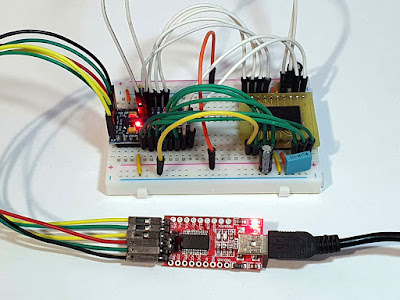
It is possible to read data from an 8-bit parallel bus NAND flash chip using the ATmega328p Arduino. Design of a SMD adapter and wiring.
NAND Flash chips are widely used non-volatile memory devices. They have high storage capacity, fast access time and are reliable, usually being able to withstand 100,000 erase/program cycles. Such chips are available with parallel or serial interface (commonly SPI). While the latter can be easily interfaced to any SPI port and can be read/programmed even by slow microcontrollers, parallel chips are faster and require more data lines (connections) to host microcontroller.
Having an old DSL modem which cannot be flashed with a locked bootloader and unavailable JTAG port I unsoldered its NAND flash. I do not own a parallel memory programmer and I do not intend to buy one for the sole purpose of dumping useless data from this flash. So, I attempted to interface this memory to what I have. At first it seemed it has too many pins to wire it to a common ATmega328p Arduino. But the datasheet revealed something else.

The flash memory I have is a 512 Mbits (64 MBytes) NAND in a TSOP48 package. Fortunately for me, NAND512W3A has an 8-bit bus width. This means both addresses and data exchanges happen on this 8-bit bus. There are some additional control lines which let the chip know what kind of information is made available through the bus. There are seven control signals and the data bus. A total of 15 wires which I can connect to an ordinary Arduino. Well, not the usual Uno since the flash is not 5 V tolerant. I had to use a Pro Mini board running at 3.3 V with an 8 MHz crystal. For the purpose of reading I guess I can spare an extra pin by mapping WP (write protect) straight to ground. All tests were done like this to avoid data corruption.
Hardware
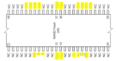
I used hot air to remove the chip from the modem board. The datasheet reveals its pin configuration:

Pin configuration of NAND512 x8 flash memory (TSOP48)
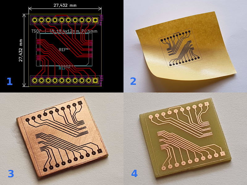
How do I put that TSOP48 SMD flash on the breadboard? Simple: with an adapter. The cheapest and fastest way to get it was to build it myself. The challenge here is to get 0.3 mm track width using toner transfer method. And I was successful. I edited the package footprint and removed all unused (NC) pins. The required pins go to usual 2.54 mm pitch pinheaders. PCB dimensions are 27.5 by 27.5 mm. The following picture summarizes the steps I took to produce it: 1. Design in KiCad; 2. Print on special paper; 3. Transfer toner to copper; 4. Etch with ferric chloride. After that I drilled the holes and soldered the pinheaders then the flash chip; finally, I put it on the breadboard and began wiring to Arduino.

The process of making a PCB for the TSOP48 NAND flash
Soldering was the most difficult part. I used a temperature controlled soldering iron with fine tip and some copper braid to remove bridges between those small pads. Besides that, with the removed pads from the footprint, I found it hard to place the chip in its correct position. Nevertheless, I succeeded.
Wiring
I put everything on a breadboard. Before plugging the USB, it's important to make sure FT232 adapter is set to 3.3 V. The NAND flash is not 5 V tolerant. There is a jumper on the PCB of the USB-Serial adapter. I set it to 3.3 V. That's why I use FT232 in the first place. It supports 3.3 V levels. Schematic is quite straightforward.

Arduino parallel NAND reader schematic
Arduino digital pins D2 to D7 are mapped to control signals. For the 8-bit I/O port I wanted to have a full 8-bit port available, but that can't be done with ATmega328p. So, pins A0 to A5 (part of PORTC) are mapped to I/O0 to I/O5. For I/O6 and I/O7 I had to use pins D8 and D9 (of PORTC). It's important to know the ports to which these pins belong since I will use direct reading/writing by accessing port registers.
Control signals
Control signals RB, R, E, W and WP are active low. With the exception of RB which should be set to input, all are outputs and their initial state have to be HIGH (inactive). CL and AL are also outputs, but these are active HIGH. In the beginning of the software algorithm, these will be set to LOW. The functions of all these pins are the following:
E- enables the chip;R- sets I/O mode to reading: NAND port is set to output; host MCU should set its port to input;W- sets I/O mode to writing: NAND port is set to input; host MCU should set its port to output;CL- command latch informs the chip that you are about to send a command (Wis actually used to latch data);AL- address latch informs the chip that you are about to send an address (Wis actually used to latch data);RB- when attempting to read the memory, the host should check this pin and wait to go HIGH if needed;WP- enables or disables write protection.
Data output to memory chip is latched on the rising edge of W. Data output is latched in no more than 35 ns after the falling edge of R and will be invalid in 15 ns after R goes high. This is quite fast for the Arduino, so I have to take care when writing the code.
If you're interested in my adapter, download here the KiCad project. In the next part I will begin writing the code for control signals and attempt to read device signature.


как прошить и прочитать Nand K9GAG08U0E?
ReplyDeleteYou can probably read data from it because it uses the same interface. But it has large capacity and you cannot dump all data in a reasonable time. You need to get a programmer.
Delete