Showing posts with label PCB. Show all posts

8-Channel relay controller with keypad and RS485 interface

 Posted by:   Posted on:    No comments

In the previous post I built a front panel with 8 push buttons which will be used to activate a module of 8 relays. Having so many I/O lines I had to come with a solution to be able to read and set each one of them with common microcontrollers. I ended up using 74HC165 for inputs and 74HC595 for outputs. These ICs are shift registers controlled using a serial synchronous protocol similar to SPI.

In this post you will see the entire outdoor unit. In the end there will be two units, the outdoor one with keypad and relays; the other is the indoor unit with Wi-Fi connectivity and MQTT capabilities. A keypad will be featured on this one too. I went with this approach because I want a robust implementation without Wi-Fi dependency. Nevertheless the keypad on outdoor unit can be remotely disabled to prevent unauthorized use. I decided to use two units after a failed design which implied the use of an ESP8266 board directly as the MCU of outdoor unit. I had problems with voltage levels (shift registers are both 3.3 V and 5 V compatible, however my relay board is 5 V only, while ESP8266 is 3.3 V only; besides that, 3.3 V applied to shift registers powered from 5 V is not recognized as digital HIGH).
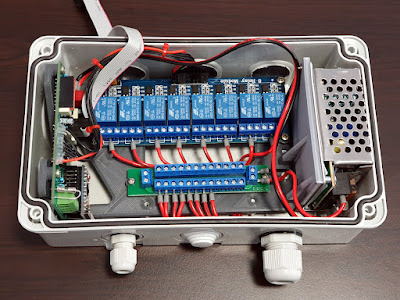
Relay controller inside plastic box

Front panel for 8-channel relay controller

 Posted by:   Posted on:    No comments

This project started from a common issue I faced while trying to interface a relay board with a microcontroller: not enough I/O pins. My purpose is to control 8 outdoor lights; therefore, I got an 8-channel relay board, powered from 5 V. But I want to add some extra functionality: this controller should have a front panel with 8 push buttons and 8 LEDs. It should also take input from sensors with digital output. So, I got 16 inputs and 16 outputs to control.

The most available solution was to use shift registers, 74HC595 for outputs and 74HC165 for inputs. Initially I thought I could use an ESP8266 microcontroller, since it would allow me to add MQTT functionality. But I had no success with this: ESP8266 is a 3.3 V microcontroller, relay board needs 5 V levels, and although shift registers can operate properly with voltages as low as 2 V, they will not recognize as high (“1”) a voltage of 3.3 V (from ESP8266) when powered with 5 V. The reason I powered them with 5 V is because relays will not be activated by 3.3 V.

Front panel fitted on the plastic cover of a wiring box

Turnkey PCB Assembly by PCBGOGO - 2022 Q3

 Posted by:   Posted on:    No comments

Modern electronic devices can only work properly if the printed circuit boards (PCBs) they are built on are reliably manufactured with high precision. PCBGOGO manufactures the best PCBs and they can meet specific client needs. It is one of the world's leading PCB manufacturers, with a production line that can provide both precision and reliability. PCBGOGO provides turnkey assembly for their customers so you can use the PCB as soon as it is delivered to you. They provide quick, professional, and reliable turnkey PCB assembly.

Turnkey PCB Assembly by PCBGOGO - 2022 Q3

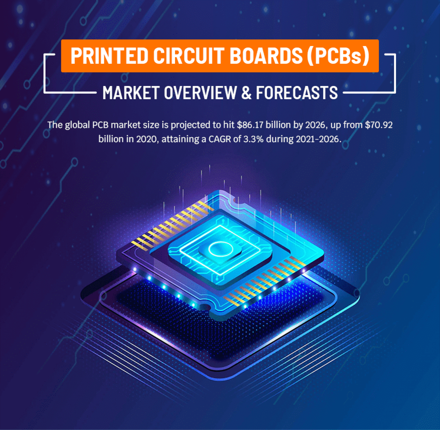
The Global Printed Circuit Board Market (infographic)

 Posted by:   Posted on:    No comments

In 2020, the Printed Circuit Board (PCB) market size was valued at around $60 billion and was projected to grow at a CAGR of more than 3% from 2021-2027.

Component miniaturization has sped off the market growth for miniaturized, lightweight, and high-performing PCBs in electronics like smart wearables, healthcare equipment, and other portable gadgets. Various Original Equipment Manufacturers (OEMs) are venturing into customized circuit board designs to improve miniaturization and obtain sleek shapes. The trend has further influenced the growth of three-dimensional printing to create compact PCBs by mounting parts on the inner layers.

The Global Printed Circuit Board Market (infographic)

PCB Layout Designing: Top 8 Tips on How to Design a PCB Layout for Beginners!

 Posted by:   Posted on:    2 comments

PCB Designing is a crucial step in a PCB Assembly Process. The printed circuit board is the project's final step, and we use it to validate a PCB prototype.

Any electronic enthusiast should have the ability to design PCB layouts if he is a pupil, an expert in the business, or a hobbyist. The construction of a proper PCB layout is an integral part of every PCB manufacturer. In this article, we'll show you the top 8 PCB Layout Design Tips for Total Beginners.

PCB Layout Designing

Making your printed circuit boards with PCBWay

 Posted by:   Posted on:    No comments

I'm quite satisfied with the PCBs I can make at home using the toner transfer method. So far, I have made PCBs for through hole devices as well as PCBs for surface mounted devices. My results are acceptable for tracks as thin as 0.3 millimeters. But there is another issue I'm having with the toner transfer method. When I apply the iron to heat the toner, the paper warps and dilates. Not too bad though. I can still solder bigger IC capsules. But what about a double sided PCB? I found it totally impossible to align top with bottom pads across the board. Until now I tried my best to keep all designs single sided by adding wire jumpers where needed.

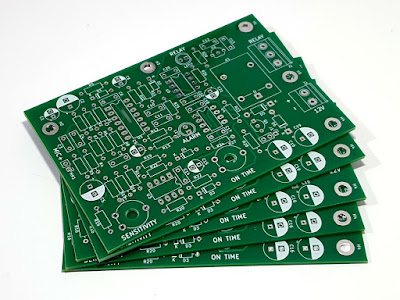
Yet when it comes to double sided PCBs or even more than two layer PCBs you need to get them professionally manufactured. Even with single sided PCBs when you want them to look professionally built or you need more pieces the right choice is a manufacturing service. I decided to try the PCB manufacturing services of PCBWay, a Chinese company which can manufacture PCBs and ship them worldwide at good prices.

PCBs ordered from PCBWay

PCBs ordered from PCBWay

Homemade PCB with toner transfer method

 Posted by:   Posted on:    1 comment

The toner transfer method is a cheap and easy way to make your own printed circuit boards (PCBs) at home. A laser printer is used to print the design on paper. Not all paper types are suitable for this kind of usage. The paper is placed with the printed side over the copper side of the circuit board and then the whole thing is heated. Most people use with good results a common iron, but if you have a laminator, use it instead of the iron. When heated, toner melts and sticks to the surfaces. The idea is to make it stick to the copper layer. After heating, the board is submerged in water and the paper should be easily peeled off from the copper side. A good transfer means no toner remains on the paper. Once this is done, the board can be etched using whatever method you want (ferric chloride for example).

This method is widespread among hobbyists because is cheap and easy. However, for some, the results are unsatisfactory and variable. I will share some of my experiences with this method.

Homemade PCB with toner transfer method incl. silkscreen

Homemade PCB with silkscreen